µISA
Overall Setup
The control unit executes microcode. It also maintains several important flags that influence the overall behavior of the processor, like whether an interrupt is currently being handled.
In general, the control unit executes one micro-instruction each clock cycle (the only exception is that memory-mapped IO accesses disable the micro-instruction counter for one cycle).
The micro-instructions are 32 bits wide and fetched from four ROM (U1 to U4) chips.
These micro-instructions then (directly or indirectly) set the control lines, or change internal state of the control unit.
The current micro-instruction is directly controlled by the following inputs:
- The 4-bit micro-instruction counter
U5. It counts up each cycle, to execute the next micro-instruction - The 8-bit opcode register
U7andU8. The opcode is fetched initially and thereby controls which control line to execute. - The 4-bit flags register
U6. Several ISA instructions should behave differently based on flags (e.g. conditional jumps), thus which specific instructions are executed depends on the flags. - The 1-bit interrupt latch
U19A. When an interrupt is pending, different microcode is executed.
These 17 bits are used as address lines into the four ROM chips which hold the microcode. Thus, they directly control the microcode word.
This also means that the execution model is fairly simple: the micro-instruction counter is incremented automatically, and can only be reset for the next instruction.
During an instruction, the only way to “jump” to another microcode location is to reload the flags.
This is used to implement sign-extension (e.g. in jcc imm8s16).
In this sense, our build differs from other 8-bit breadboard computers.
Ulf Casper’s build, for example, has two “layers” of microcode ROMs:
 The advantage of such a design is that the first layer can pre-decode the instruction (e.g. decide whether a jump is executed or not).
Not having to feed five flags (SZVC plus interrupt) into the second layer comes with greater flexibility.
The advantage of such a design is that the first layer can pre-decode the instruction (e.g. decide whether a jump is executed or not).
Not having to feed five flags (SZVC plus interrupt) into the second layer comes with greater flexibility.
This flexibility can be used for longer instructions as well as jumps inside the microcode, which in turn enable implementing complex instructions like reading n bytes from the serial interface to memory.
Our approach on the other hand is much simpler.
With “only” four microcode ROMs, it needs less physical space.
Furthermore, it enables us to make the high-phase of the clock very short.
There only needs to be enough time for the ripple carry of the address latch counter (after loading in the first half-cycle), which is way less than the ~70 ns needed for the flash outputs to settle.
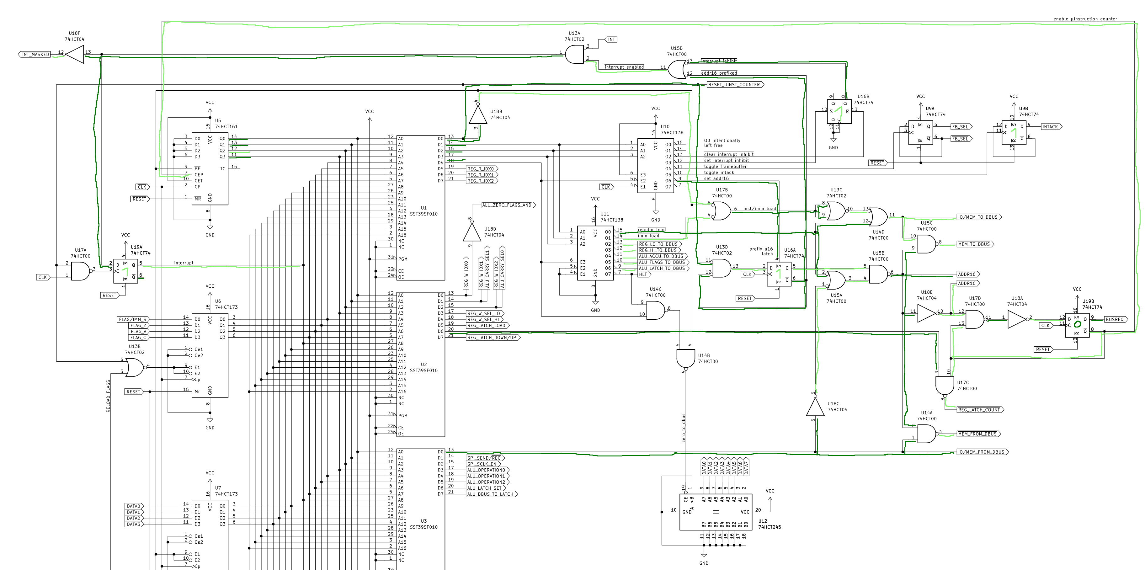
Overall we have an 8-bit instruction register, a micro-instruction counter and flag register. These inputs go into the four ROM chips. With the inputs they determine which control lines should be set. Sometimes we have to combine several outputs of the ROM chips to get a control signal. The outputs are then going to the other modules of the processor.
It should be noted that the registers / latches controlling the inputs to the microcode ROM are attached to the inverted clock. For more details refer to the clock documentation.
Timing-wise there are several scenarios for which correctness is not obvious.
For example, when a new opcode is fetched into the instruction register, this happens on the falling (normal) clock edge.
Immediately afterwards, the instruction register changes. This causes control lines to change too, so that the value on the bus is no longer the value fetched from memory, but something else instead.
While this seems bad, it is actually not an issue, because the instruction register update is the first thing that happens on falling edge, and it takes a few nanoseconds for the changes to propagate, which is sufficient.
Internal State
There are several internal flip-flops that control various parts of the processor state:
U13Dstores theprefix_a16state. If this is enabled, then memory is loaded from IO space instead of normal RAM. This is clocked on falling edge.U16Bstores theinterrupt_inhibitstate. When interrupts are inhibited, they do not occur. It is a set-reset latch, with both inputs being control lines.U9Astores thefb_selstate. This switches between the two GPU framebuffers. It is so clocked by a control line.U9Bstores theintackstate. The interrupt routine enablesINTACK, then reads the interrupt, and then disables it again. It is clocked by a control line.U19Bstores thebusreqstate. Whenbusreqis enabled, the clock is held for a tick, so that IO devices have time to write something to the bus. Then, it disables itself again. It is also clocked on falling edge.U3Bof the clock module stores theimm_signstate. This is the highest bit of the last 8-bit value loaded from memory.
Additionally, there are several registers and latches which control the microcode address, updated on rising clock. These are already documented above.
Each operation can be understood on its own. Unfortunately, they also interact in several nontrivial ways.
For example, when executing an instruction with the prefix_a16 enabled, an interrupt should not happen, because otherwise the interrupt handler would need to unset and restore the prefix_a16 flag so that the instructions don't notice that it was interrupted. Thus, interrupts are disabled when prefix_a16 is high so that this does not need to be handled.
The interaction between busreq and prefix_a16 is most peculiar since busreq stops the micro-instruction execution for one cycle and only ever happens when the prefix_a16 latch is enabled. It is described in further detail below. Both are transient and reset at the end of the current instruction, except if set while executing the instruction fetch, then they persist to the next instruction. This is how the a16_prefix instruction works, which modifies the next opcode to load from IO space.
The interrupt_inhibit flag is set by the interrupt handling microcode and cleared by the iret instruction.
Further, the cli and sti instructions can control it directly.
The intack flag is also set by the interrupt handling microcode. That microcode enables it briefly and then immediately disables it again.
From Control Words to Control Lines
A control word, or microcode instruction, is 32 bits wide. Yet, there are more than 32 control lines exiting the control unit, as well as several which are internal to the control unit. The control logic decodes the control word into control lines, while also incorporating the state of internal flip-flops.
Of the 32 available bits in a control word, one is unused (or rather, it currently drives the assert LED, for debugging purposes). 20 control word bits are directly driving control lines, which leaves 11 control word bits to decode to other control lines. For this, we use several techniques:
- We identified three pairs of control lines where one control line is always “do not care,” i.e. because the control line would control which register is written to, but no register write is actually happening. Thus, one control word bit suffices for each such pair. We call these “mutually ignoring.”
- Four control word bits are fed into a 4-to-16-bit decoder, which allows these 4 bits to drive 16 different control lines, as long as there is only ever one such control line active.
In practice, many control lines are mutually exclusive, for example those that control writing onto the bus, since there may only ever be one device writing onto the bus.
Further, some of these 16 control lines also indirectly set other control lines.
Note however that some actions such asset_addr16need to be performed along with the instruction fetch, so we cannot useimm_loadhere. This is whyRESET_UINST_COUNTERautomatically activatesMEM_TO_DBUS. - Two control word bits, namely
RESET_UINST_COUNTERandRELOAD_FLAGS, control the internals of the control unit. - The
reg_latch_countcontrol word bit drives the~REG_LATCH_COUNTcontrol line, except that it is gated behind an NAND gate so that it does not happen during a bus request (see here). - The
IO/MEM_FROM_DBUScontrol line also indirectly affects one other control lines.
More information on how each control line is formed can be found in the documentation on control lines. The control lines involved in a bus request are also described below.
Modifying Internal Control Unit State
We now discuss how a control word can affect the internal state of the control unit, by discussing all the relevant control words:
RESET_UINST_COUNTERresets the counter, and also reloads the instruction, flags, and interrupt register in the control unit. It is executed during the instruction fetch phase, and terminates the current instruction to start executing the next instruction.clear_interrupt_inhibitandset_interrupt_inhibitdirectly affect the state of theinterrupt_inhibitlatch. When this is set, pending interrupts will not be propagated to theinterruptlatch, i.e. they will not trigger.toggle_framebufferswitches between framebuffers.toggle_intacktoggles theintacksignal on and off. It is used during interrupt handling, see below.set_addr16sets theaddr16flag. It is reset the next timereset_uinst_counterhappens. If bothreset_uinst_counterandset_addr16are enabled, then the latch remains set.RELOAD_FLAGSis used when an instruction needs to adapt to potentially updated flags during its execution. This loads the current value of the flags from the ALU into theflagsregister, similar to instruction fetch. However, the other registers are not affected, and in particular the counter is not reset, so that the instruction can now continue.
Note thatRELOAD_FLAGSloads slightly different values into the flags than the normalRESET_UINST_COUNTER. First, it can optionally select the shadow carry flag, by assertingALU_USE_SHADOW_CARRY. Further, to implement sign-extension, we sometimes want to execute different microcode depending on the sign bit of the immediate. For this, thereload_flagsmechanism does not actually load thesignflag into the control module’s copy of the flag register, but instead loads the sign of the last 8-bit value loaded from memory, stored inimm_sign(see the clock schematic).
Resets and Interrupts
The microcode for interrupts and for reset is discussed in detail in the documentation on microcode.
On reset, the microcode at microcode ROM index 0x00000 starts executing. This jumps to program address 0x0000 and zeroes the accu, the flags, and the stack pointer. It also inhibits interrupts.
The interrupt thus jumps to the start of the ROM with the interrupt number (0x01-0xff) is in the accu register.
Note that 0x00 is the interrupt number for reset, which should not occur as it is used internally. We want the interrupt handlers to be customizable by each program, so we dispatch them from a table at 0x1000 by convention. Hence, any actual program located in memory should start with something like this:
    cmp acc, 0
    je is_boot
    ... ; calculate interrupt table index
    ... ; call interrupt handler
is_boot:
    ; ...
Within the interrupt handler, all user ISA registers except acc, the flags, and the PC are interrupt-handler-saved, i.e. the interrupt handler must save and restore them manually.
Note that the stack pointer is not saved microarchitcturally, so we save registers to the user stack if we're clobbering them in an interrupt handler.
We do not reserve a red zone and user software should thus expect that values below the stack pointer could be overwritten at any time by an interrupt handler.
Bus Requests and Memory Accesses
Our CPU has 16-bit wide memory addresses. It also has a 16-bit IO memory space that is accessed using normal memory instructions, when the prefix_a16 instruction is executed beforehand. This prefix instruction ensures that the prefix_a16 latch is set during the execution of the next instruction. Conceptually, we can consider this a 17-bit memory space, where the highest bit controls whether we access IO memory or regular memory.
During a normal (i.e. not IO) memory read, the IO/MEM_TO_DBUS and MEM_TO_DBUS lines are active (note that some of them are active-low), while ADDR16 is inactive.
BUSREQ will not be enabled, and the memory read continues normally.
During a regular write, both IO/MEM_FROM_DBUS and MEM_FROM_DBUS will become active.
If the next instruction is a memory instruction, but prefix_a16 is set, it will not access regular memory, but IO memory. For this, it may execute a bus request, which means that the memory access takes two cycles, so that IO devices have time to react. This is what happens when a load from/store to IO memory takes place, e.g. if regular_load is set and the prefix_a16 latch is set. This also happens during interrupt processing, since the interrupt number is presented as the value stored in IO memory address 0. We now describe what happens during such a bus request, by looking at line 5 and 6 of the interrupt handling.
The Interrupt Example
The state at the beginning of step 5 (line 16-17) in the interrupt handling is visualized in the following picture.
The situation here is that the control lines have stabilized, while the (normal) clock is still low.
In the next half-cycle, it will go high, and the busrequest latch will become 1, enabling the bus request.
This will further stop the microinstruction counter from counting, and hence after another cycle, BUSREQ will go low again while none of the other control lines change.
This gives the IO devices enough time to react to a bus request.
Once the BUSREQ line is low again, the micro-instruction counter continues as if nothing has happened.
In particular, all of this is transparent to the microcode.
In this picture, logically high lines are marked in light green, while logically low lines are dark green.
Not marked lines can be ignored. In particular, the interaction between the a16_prefix latch and the BUSREQ latch is noteworthy.
What the Example Does Not Show
It can be seen that REG_LATCH_COUNT is gated by the BUSREQ flag.
This is because we sometimes want to do a bus request while also increasing the address latch.
However, since the micro-instruction counter here is stopped for one cycle, the control word is executed twice.
Consequently, we would also increase the address latch twice, which is not intended.
Thus, the corresponding line is gated so that it is only enabled once during a bus request.
There are other potential control word combinations that might cause similar issues (i.e. the ALU might add twice), but they do not occur in practice.
Further, it can be seen that a write operation to IO memory differs from a write operation to normal memory only by not setting MEM_FROM_DBUS.
Thus, IO devices must consume writes quickly, since they only take one cycle.
Even further, there is imm_load, in contrast to regular_load.
This control line, is OR'd with the RESET_UINST_COUNTER control line to determine when a load is happening that is an instruction fetch.
Since instructions should never be fetched from IO memory, this bypasses all the logic for IO memory accesses and simply accesses normal memory.
Finally, the same can happen during a write operation.
LEDs Used in the Build
- The flags are visualized on the vertical board with four green LEDs. The order is SZVC (from left to right).
- The LEDs for the instruction register are currently on a separate breadboard. The MSB is on the left.
- The µInst counter is visualized on the vertical board with four red LEDs. The MSB is on the right.
- The green LED next to the µInst counter is on iff the µInst counter is enabled.
- The assert LED located next to U3 indicates that an
assertzinstruction failed.