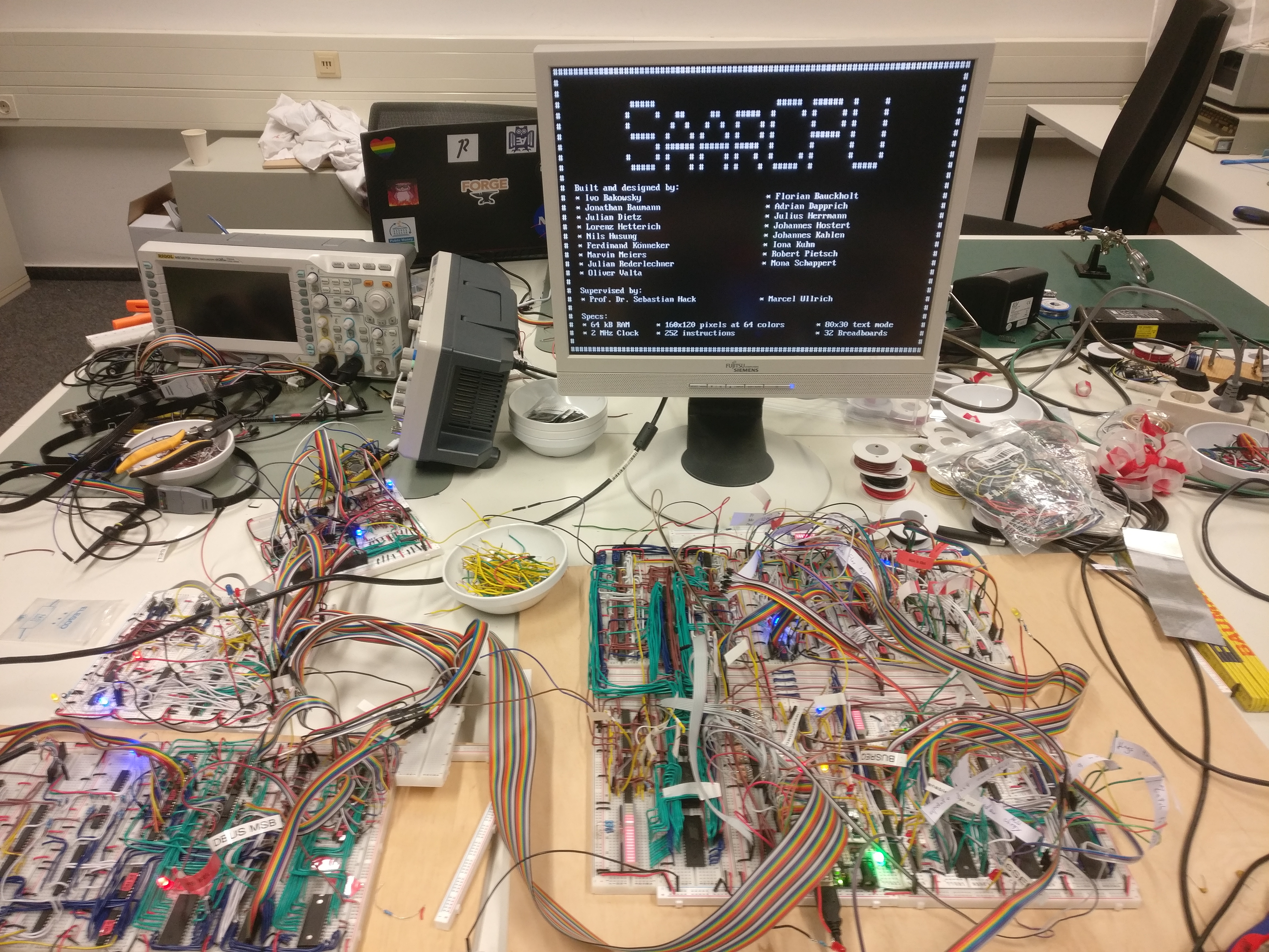
About the SaarCPU
Although the name suggests otherwise, SaarCPU is a complete eight bit computer built using 74HCTxx logic chips on breadboards. The project was conducted as a seminar at Saarland University supervised by Prof. Sebastian Hack and Marcel Ullrich from the Compiler Design Lab.
The processor was built by Ivo Bakowsky, Florian Bauckholt, Jonathan Baumann, Adrian Dapprich, Julian Dietz, Julius Herrmann, Lorenz Hetterich, Johannes Hostert, Nils Husung, Johannes Kahlen, Ferdinand Könneker, Iona Kuhn, Marvin Meiers, Robert Pietsch, Julian Rederlechner, Mona Schappert, and Oliver Valta.
Project goals
The project was initially inspired by Ben Eater's 8-bit computer build and has been designed to have the following features:
- ALU for 8-bit operations
- Register file with 16 8-bit registers
- 16-bit addressable memory (64 KiB)
- Interrupt handling
- I/O device interfacing (PS/2)
- VGA Graphics
Final design
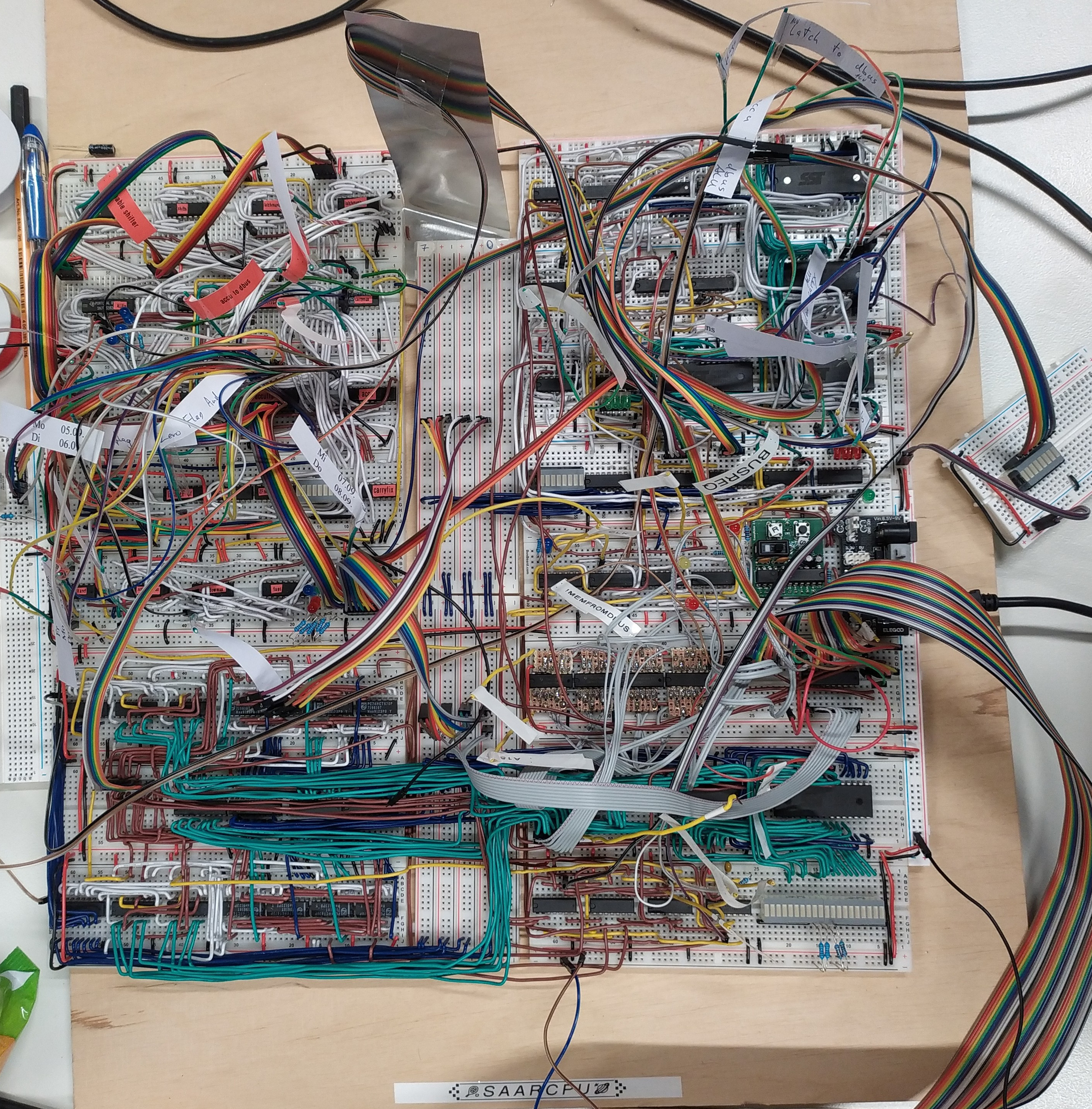
We split the hardware of our processor in six different subgroups: Control, Registers, Memory, Arithmetic Logic Unit (ALU), Peripherals (I/O) and Graphics. Most modules are connected via an 8-bit data bus, and I/O, Graphics and Memory are additionally connected to the 16-bit address latch within the register unit.
- The control unit is the heart of the processor. It contains the system clock and decodes ISA instructions into sequences of control signals sent into other components.
- The ALU does basic calculations on single data words like arithmetic or boolean operations. Doing these, it also sets flags influencing the behavior of the control unit in a therefore-reserved flag register.
- The register file provides a set of small but quickly-accessible data buffers that are mainly used to provide and hold ALU operands and results.
- In addition to the main system, we have created several peripherals like a PS/2 keyboard controller, a SD card adapter and an interface for communication with an Arduino microcontroller.
The graphics unit produces a VGA display signal. For that, it contains two frame buffers that can be filled with text and pixel graphics.
Implementation
We built the main parts of the computer on two columns of eight breadboards with an 8-bit data bus and shared clock lines in between as can be seen in this layout diagram:

In addition to the main computer, we also built a VGA graphics module and interfaces for several I/O devices. These are located on separate breadboards and can be connected to the CPU via the interface board.
A more detailed description can be found on the corresponding part pages and in the following section.
Timeline
We started working on this processor in May 2022. Before designing the first circuits, we discussed different existing designs both from 80s commodity CPUs and other hobby builds (a list of the considered ones can be found in the references) and drafted a basic instruction set architecture. Having done these fundamentals, we split our student group into teams planning and constructing specific components. By June 2022, every team started to design and then build their component. To discuss progress and for major decisions affecting multiple components, we had regular meetings. These big meetings by themselves were not sufficient, so we frequently had smaller meetings with representatives from two or three teams to discuss interactions between the components. After construction every unit was tested individually by the team with simulating the other components with an microcontroller (e.g. Arduino or self-built testing circuits). In the beginning of September, all components were ready for integration into the final build. We combined components part by part and after every step, we tested that the parts work together as expected. By late October, we finished integration testing and wired each part up for our final processor design.
Simultaneous to the hardware construction, many team members also developed software (e.g. an assembler, an emulator and a simulator for the microarchitecture) for testing, debugging and finally using the processor.
Future Work
Here's some of the topics we initially discussed, but have not had time to explore yet.
A proper software suite
During the seminar, we were mostly busy with actually building the computer. The baby steps we achieved were ultimately hand-coded in assembly and flashed directly to the ROM chip.
A C compiler toolchain targeting our custom ISA would be great. We experimented with a custom LLVM backend, but it turns out that LLVM's support for weird 8-bit architectures is not great, while also being way too complicated for everything. We pose that modifying sdcc might be the way to go here.
In addition to a compiler toolchain, some simple application scaffolding would be nice. We're currently flashing ROM chips each time we update code or test a different feature. Instead, we'd like to have a static "Boot-ROM" that loads externally provided code via a simulated IO device. Features like check-summing, some fixed standard routines, and boot menus would also be nice. :)
SaarPCB
Bringing SaarCPU to the masses — or even just over to your friends' — is not practical with a fragile mess of connected breadboards. We initially discussed the idea of prototyping a custom PCB with our CPU design. PCB prototyping services make this possible and even seem to stock 74xx ICs for factory pick-and-placing.
An ISA-like design with separate cards for each major component on a shared bus might be the way to go here.